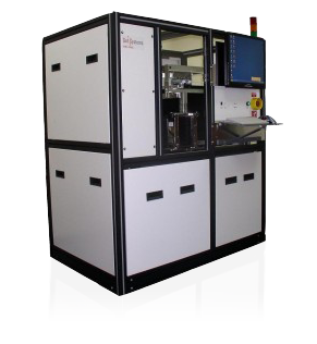
Product description:
TIM200/300S is automated defects macro inspection tool for the Semiconductor industry. The TIM-200/300S is using a unique and smart technologies for macro defects inspection at a very low cost. The tool is able to detect large variety of wafer defects in the defined size limit.The main idea of the tool is to capture in one shot the wafer surface and analyze the full captured image. This unique method differs from traditional methods that using wafer scan methodology.
The system is using Bright field and Dark field methodologies for both front side and back side of the wafers and is also able to detect defects at the wafer edge.The tool is able to deliver high productivity broadband defect inspection capability, enabling high sensitivity in production, increased sampling for tighter process control together with lower cost of ownership.
Tool can be used as integrated or stand alone.
Main Technology Highlights:
Unique light source methodology allowing user to pinpoint the defects in the vision light spectrum. This exclusive high-brightness light source enables new optical modes that deliver increased resolution and contrast for capturing a broader range of yield-critical defect type.
Wafer image acquiring is being performed in one shoot that makes the machine working very fast while inspecting 100% of processed wafers.
The Smart Algorithm is based on the leading edge aviation technologies developed by May HTS engineers.
Applications:
The tool is able to detect various type defects found in front side, back side and in the edge of the wafer created during wafer processing in the fab: Metallic, Litho, SOI, Etch, Cracks, Scratches, Roughness, Handling, Probing and bumps, end of line defects.
Tool Specifications:
- Designed to operate in clean room class 1
- Inspection Mode : Automated, 100% wafer’s surface macro inspection
- Inspection method : Bright field – wafer front side and back side, Dark field – wafer front side and back side.
- Minimum defect size : ~20u
- Wafer size : 200 or 300mm
- Throughput: up to 160WPH
- Wafer transfer: Robotic handler
- FAB Host communication : SECS/GEM Protocol
- Cassette barcode reader : Option
- Alignment: Wafer Notch alignment
- Number of load-ports: 1 (2 option)
- Foot print: 135X87cm (300mm)